
Multilayer PCB
For complex designs that need stable signals, dense routing, and solid layer-to-layer connections.
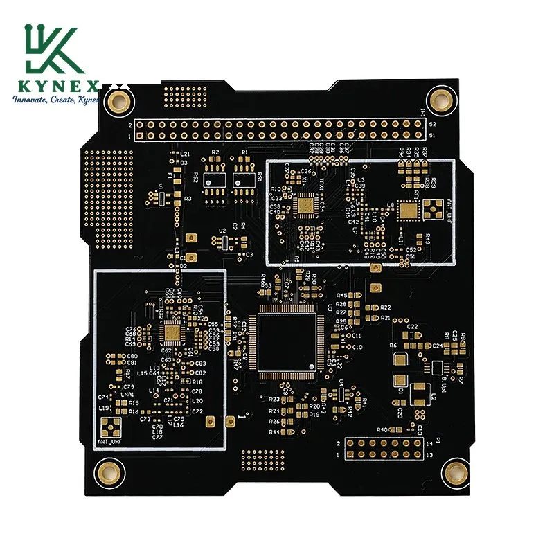
| Layers | 2–32 |
|---|---|
| Line / space | 0.065 mm minimum |
| Material | FR-4, high-Tg |
| Surface finish | ENIG |
| Process | Max. panel 558 × 670 mm, up to 210 µm copper in pattern |
| Testing | Flying probe or electrical test |
General capability of our current production. Final limits depend on your stack-up and design review.