About Us
KYNEX Electronics is a professional PCB and PCBA manufacturer based in Shenzhen, China, established in 2010.
Who we are
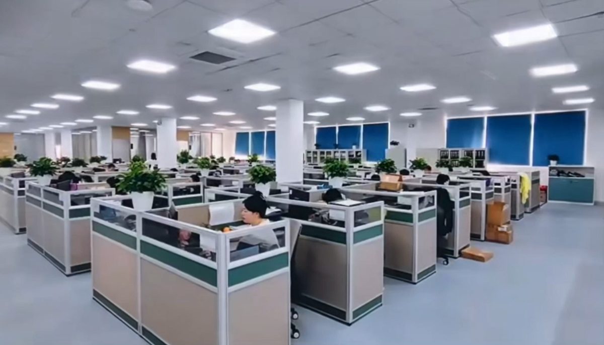
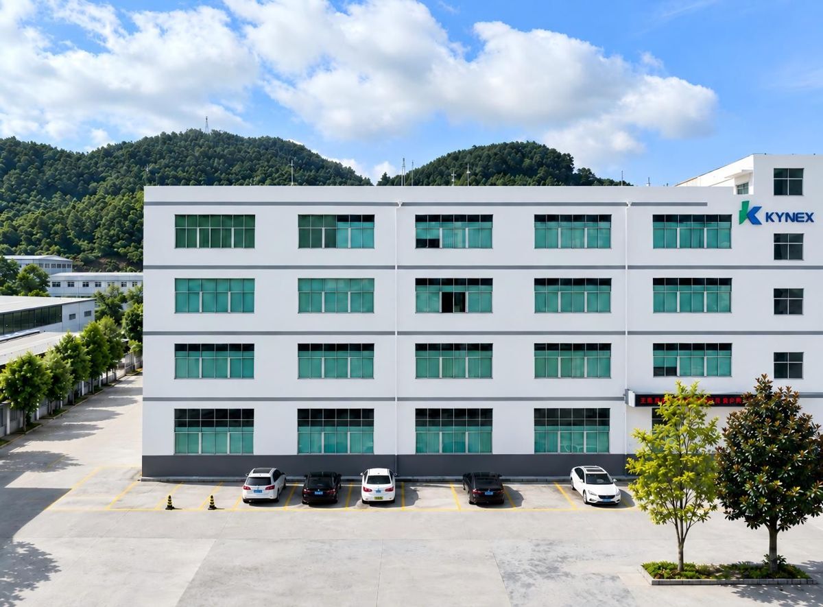
Since 2010 we have focused on PCB manufacturing, engineering, quality management, and customer service. Our facility covers more than 5,000 square meters with over 600 employees, including more than 100 professionals in PCB design, process, engineering support, and quality control.
What we do
Multilayer, HDI, high-frequency and high-speed, high-Tg, heavy copper, metal core, rigid-flex, mixed-dielectric, and customized PCBs, plus PCB assembly (PCBA). Used in telecommunications, industrial control, consumer electronics, power electronics, medical equipment, automotive, energy, and aerospace.
How we work
Strict quality control runs through the whole process: incoming material inspection, engineering review, production, testing, final inspection, and shipment. Our engineers support product development, process optimization, and manufacturing problem-solving.
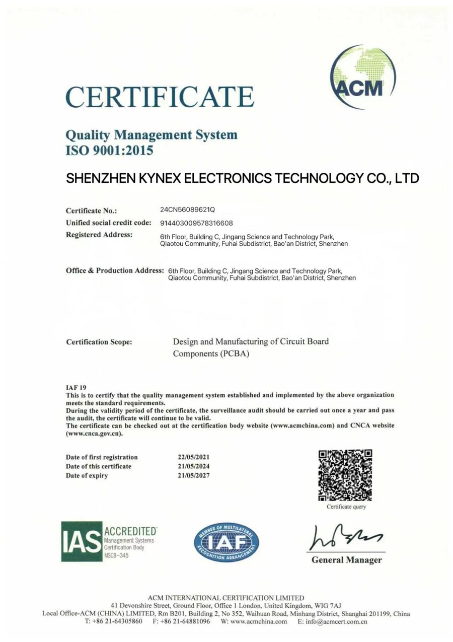 ISO 9001:2015
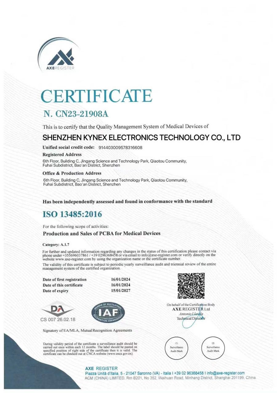 ISO 13485:2016
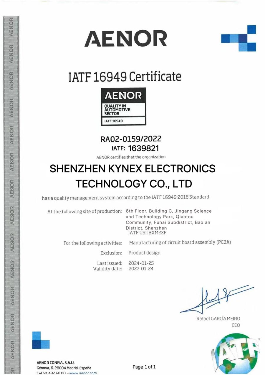 IATF 16949:2016
One-Stop Manufacturing Services
Engineering, sourcing, assembly, and delivery in one connected workflow.
PCBA Design
Software and hardware engineering support.
Turnkey PCBA
Component selection, BOM sourcing, and purchasing.
SMT Assembly
SMT, DIP, programming, testing, and repair.
Product Assembly
Assembly, aging, packaging, and shipping.
Standards & Compliance
- Quality and environmental management systems: ISO 9001, ISO 14001, ISO 13485, and IATF 16949
- Products and processes comply with UL, RoHS, CE, FCC, and other applicable regulations
Quality Assurance
Inspection at every stage, from incoming materials to finished products.
Incoming inspection
Materials and component checks.
In-process control
SPI, AOI, and X-ray inspection.
Final validation
Functional testing and final checks.
- Printing Cpk > 1.33
- Post-reflow PPM < 200
- QA first-pass yield > 99%
- Customer line defects < 1,000 ppm
- Customer satisfaction > 90
Production Process
From quotation and incoming material inspection to packaging and logistics: 24 steps with inspection built in.
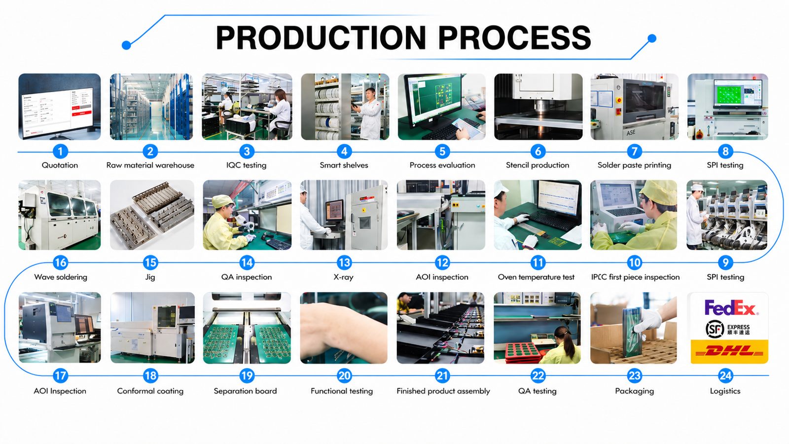
- SMT: incoming materials, IQC and storage, paste printing and SPI, placement and first article, reflow, AOI, and X-ray
- DIP: board loading, component insertion, first article and AOI, wave or manual soldering, inspection and QA
- Final: programming, functional testing, aging and coating, final QC and QA, ESD packing and storage
- Nonconforming material or assemblies return to inspection or repair before release
SMT / PCBA Capability
From BOM sourcing to tested, assembled PCBAs.
- SMT, DIP, programming, testing, repair, coating, assembly, and packaging
- Solder paste printing accuracy ±0.025 mm, placement accuracy ±0.05 mm
- PCB thickness 0.4–4 mm, components from 0201 up to 45 mm, minimum BGA / IC pitch 0.35 mm
- Max. SMT board size 400 × 510 mm
- 10-zone lead-free reflow with ±2 °C accuracy
- AOI, X-ray inspection, and BGA rework
- Lead time 3–5 days when materials are ready
Production Equipment
Precision placement, inspection, and assembly.
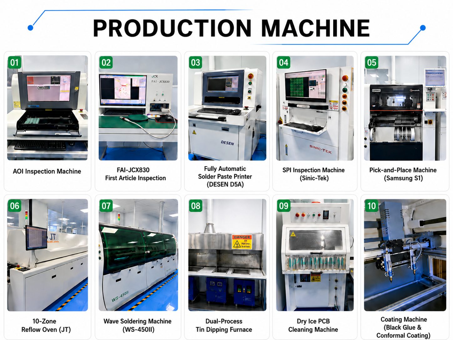
- High-speed pick-and-place machines (Samsung S1)
- Fully automatic solder paste printers (DESEN D5A), SPI inspection machines (Sinic-Tek)
- AOI inspection machines and first article inspection (FAI-JCX830)
- 10-zone reflow ovens (JT), including nitrogen ovens
- Wave soldering machines (WS-450II) and dual-process tin dipping furnaces
- X-ray inspection systems and X-ray component counters
- Dry ice PCB cleaning machines, coating machines (black glue and conformal coating), PCB routing machines, BGA rework station
- Automatic programming machines, CNC engraving, heat shrink, Wi-Fi, 4G module calibration, and battery test equipment
R&D and Laboratory
Engineering support from requirements to a production-ready prototype.
Engineering support
PCB / PCBA design and technical review.
Prototype development
2–32 layers, HDI, rigid-flex, and advanced PCB solutions.
Testing & validation
Electrical, functional, and reliability testing.
- Electrical: LCR meter, spectrum analyzer, electroacoustic device analyzer, ESD simulator, Bluetooth tester, transistor curve tracer, line impedance stabilization network, high-magnification microscope
- Reliability: thermal shock chamber, temperature and humidity chamber, salt spray chamber, aging and life test chamber, vibration tester, RoHS analyzer, 2D optical measuring system, variable-frequency power supply
- Durability: drop tester, cable flex tester, insertion and extraction force tester, AC withstand voltage and insulation tester, RCA tape, alcohol, and pencil hardness abrasion testers, constant-temperature water bath
Applications We Serve
- Telecommunications
- Industrial automation and control
- Consumer electronics and smart home
- Robotics
- Security
- Medical and beauty devices
- New energy and energy storage
- Automotive electronics
- Power electronics
- Aerospace
Selected Projects
Turnkey PCBA for medical, energy storage, sensor, industrial, and consumer products, and complete product assembly.
- Smart pet water fountain
- High-speed hair dryer
- MUZEN audio
- Hair removal device
- Commercial robot
- Pool-cleaning robot
Facilities, Exhibitions & Team
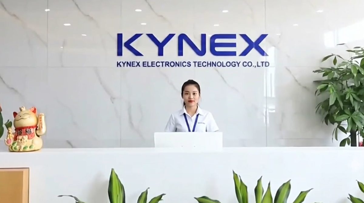
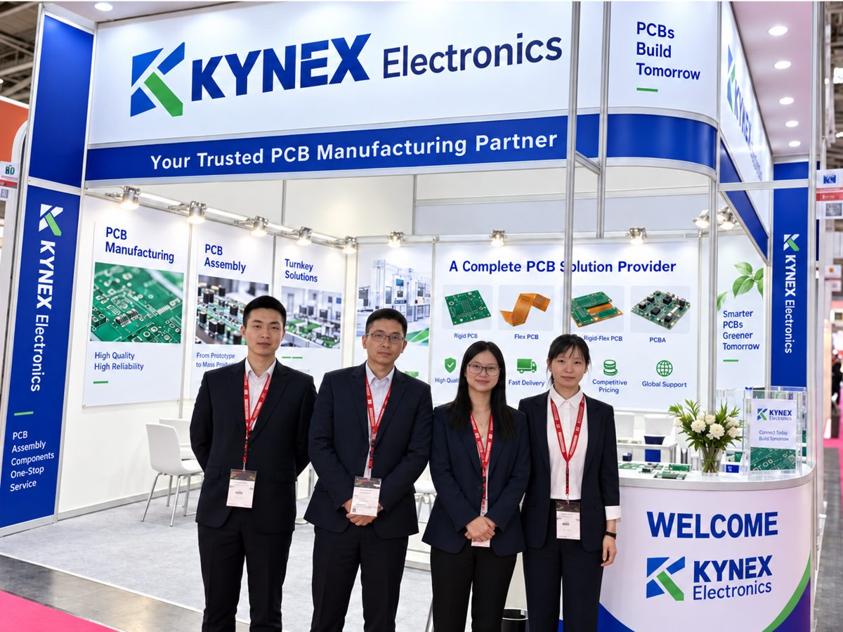
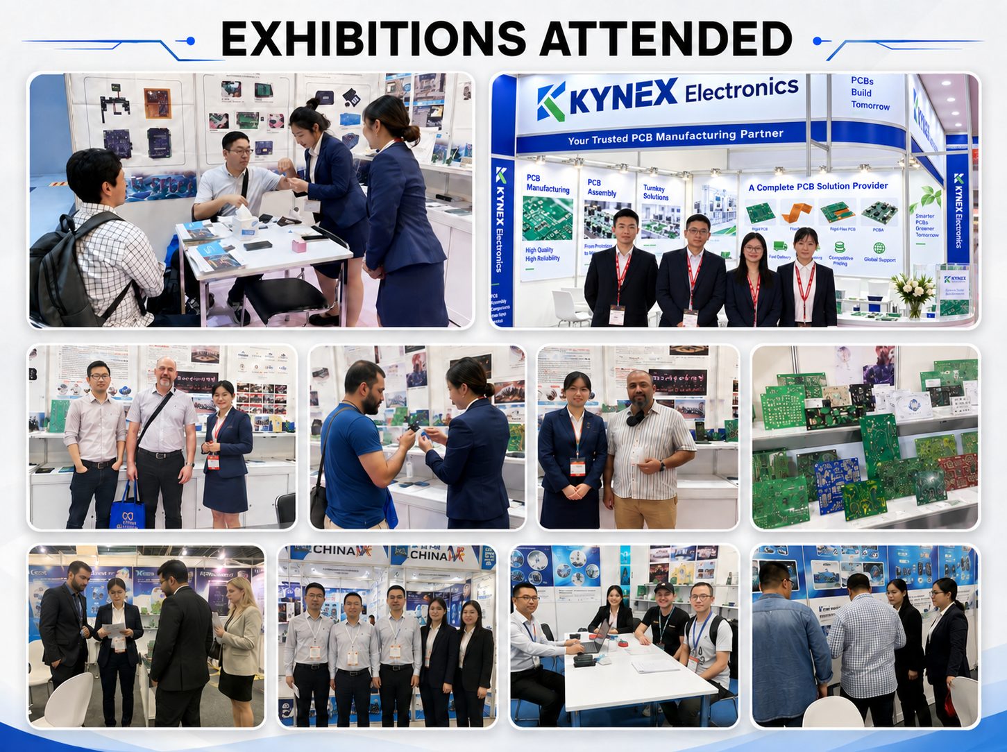
Our reception, office, trade-show presence, and the people behind the boards.